All ABOUT DIODE

Diode is a two-terminal electronic component with asymmetric conductance , it has low (ideally zero) resistance to current flow in one direction, and high (ideally infinite) resistance in the other. Today most diodes are made of silicon, but other semiconductors such as selenium or germanium are sometimes used. A semiconductor diode, the most common type today, is a crystalline piece of semiconductor material with a p–n junction connected to two electrical terminals.

image


FUNCTIONS

The most common function of a diode is to allow an electric current to pass in one direction (called the diode’s forward direction), while blocking current
in the opposite direction (the reverse direction). This unidirectional behavior is called rectification, and is used to convert alternating current to direct current, including extraction of modulation from radio signals in radio receivers—these diodes are forms of rectifiers .

Symbol of diode

image

CONNECTING DIODE PROPERLY

I hope you understand the positive and negative terminal of diode.
image

DIFFERENT TYPES OF DIODES

There are different types of  diodes and each of them have different function.

Zener diodes are used to regulate voltage.

avalanche diodes are used to protect circuits from high voltage surges.

varactor diodes are used to electronically tune radio and TV receivers.

tunnel diodes , Gunn diodes, IMPATT diodes are used  to generate radio frequency
oscillations.

light emitting diodes(LED) are used to produce light.

We will be using LEDs and photodiode or LDR in our projects, so here is the note on two. To know more about LED check out my Light Emitting Diode (LED) post or Connecting LED Properly post, to know more about LDR click here

Light-emitting diodes (LEDs)

In a diode formed from a direct band-gap semiconductor, such as gallium arsenide, carriers that cross the junction emit photons when they recombine with the majority carrier on the other side. Depending on the material, wavelengths (or colors) from the infrared to the near ultraviolet may be produced. The forward potential of these diodes depends on the wavelength of the emitted photons: 2.1 V corresponds to red, 4.0 V to violet. The first LEDs were red and yellow, and higher- frequency diodes have been developed over time. All LEDs produce incoherent, narrow- spectrum light; “white” LEDs are actually combinations of three LEDs of a different color, or a blue LED with a yellow scintillator coating. LEDs can also be used as low-efficiency photodiodes in signal applications. An LED may be paired with a photodiode or phototransistor in the same package, to form an opto- isolator .

Photodiodes

All semiconductors are subject to optical charge carrier generation. This is typically an undesired effect, so most semiconductors are packaged in light blocking material.
Photodiodes are intended to sense light( photodetector ), so they are packaged in materials that allow light to pass, and are usually PIN (the kind of diode most sensitive to light). A photodiode can be used in solar cells , in photometry, or in optical communications . Multiple photodiodes may be packaged in a single device

Most popular 1N-series diodes

We will be using 1N-series diodes. The standardized 1N-series numbering EIA370 system was introduced in the US by EIA/JEDEC (Joint Electron Device Engineering Council) about 1960. Among the most popular in this series were:
1N34A/1N270 (Germanium signal),
1N914/1N4148 (Silicon signal),
1N4001 -1N4007 (Silicon 1A power rectifier) and
1N54xx (Silicon 3A power rectifier)

If you want to know more about diode let me know it through the comments.

SPEAKER

A loudspeaker (or “speaker”) is an electroacoustic transducer that produces sound in response to an electrical audio signal input. Non-electrical loudspeakers were developed as accessories to telephone systems, but electronic amplification by.vacuum tube made loudspeakers more generally useful. The most common form of loudspeaker uses a paper cone which is vibrated by an attached voice coil electromagnet between the poles.of a permanent magnet, but many other types exist. Where high fidelity reproduction of sound is required, multiple loudspeakers may be used, each reproducing a part of the audible frequency range. Miniature loudspeakers are found in devices such as radio and TV receivers, and many forms of music players. Larger loudspeaker systems are used for music, sound reinforcement in theatres and concerts, and in public address systems.

Here is the picture of a 8R speaker we which we will be using in our project.

image

Symbol of speaker
image

The most common type of driver, commonly called a dynamic loudspeaker, uses a lightweight diaphragm , or cone , connected to a rigid basket, or frame, via a flexible suspension, commonly called a spider, that constrains a voice coil to move axially through a cylindrical magnetic gap. When an electrical signal is applied to the voice coil , a magnetic field is created by the electric current in the voice coil, making it a variable electromagnet. The coil and the driver’s magnetic system interact, generating a mechanical force that causes the coil (and thus, the attached cone) to move back and forth, thereby reproducing sound under the control of the applied electrical signal coming from the amplifier .

Modern driver magnets are almost always permanent and made of ceramic, ferrite, Alnico, or, more recently, rare earth such as neodymium and Samarium cobalt. The size and type of magnet and details of the magnetic circuit differ, depending on design goals.

HOW TO CONNECT ELECTRONIC COMPONENTS

Here is a quick post on how to connect the basic electronic components correctly. These are cuts from my earlier post. This post is due to a suggestion  from my friend. He thought that a post like this can be used for quick reference and will be helpful to the starters. If you want to knew more about each components check out my other posts.

CONNECTING LED

A LED is a two-terminal electrical component, to identify them

Positive terminal can be identified as the longer leg and shorter leg is the negative terminal.
                         OR
If you look inside the LED you can see two small lead, fat one looks like a flag which is the cathode (negative) and other one looks almost straight which is the anode (positive). The symbol of LED is:-

image

CONNECTING RESISTOR

A resistor is a two-terminal electrical component

Resistor can be connected either way, that means it have no positive and negative terminal. Both symbols below are used to represent resistor in a circuit diagram. You can use any one of the two symbols:-

image

CONNECTING CAPACITOR

A capacitor is a two-terminal electrical component.

The ceramic capacitors can be connected either way, that means it have no positive and negative terminal. The symbol used for the ceramic capacitors in a circuit diagram is:-

image

The electrolytic capacitors have a positive terminal (longer leg) and negative terminal (shorter leg). The symbol used for the electrolytic capacitors in a circuit diagram is:-

image

CONNECTING LDR

LDR is also a two-terminal electrical which can be connected either way, that means it have no positive and negative terminal. The symbol of LDR is :-

image

CONNECTING NPN BJT
                                                  
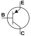
I have marked the  collector (C), base (B) and emitter (E) pins on a real NPN BJT and also on the symbol

image

CONNECTING PNP BJT

I have marked the  emitter (E), base (B) and collector (C) pins on a real PNP BJT and also on the symbol

image

CONNECTING 555 TIMER IC

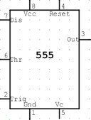
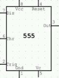
For connecting 555 timer check out this post The 555 timer IC pinout. I have marked each pin on a 555 timer IC and here is the symbol of 555 timer IC:-

image

Electronic Symbols | Schematic symbols

This post is for the starters out there who is having trouble in understanding the symbol of the circuit. I should have added this post before getting in to projects, here it is because of the request from my friend. I will add new symbol as we use them in our circuits. If you want more symbol OR have doubts on symbols, just leave a comment and I will help you.

RESISTOR

image

CAPACITOR
        1.electrolytic capacitor

image

        2. Ceramic capacitor

image

LED

image

BATTERY

image

LDR

image

555 TIMER IC

image

PNP TRANSISTOR

image

NPN TRANSISTOR

image

SPEAKER

image

SWITCH
     

image

PUSH SWITCH

image

GROUND CONNECTION

image

DIODE

image

CONNECTING LED PROPERLY

It’s important to connect a LED the correct way in a circuit because LED shows the output in many of the circuit that we are going to discuss. LED is simple to connect – once you know how.
I thought that it is important for starters to connect a LED in the proper way. This post is only to show how a LED can be connected to batteries without damaging it.

Let’s look into three example of connecting LED. I took these three example because all three situation can happen when you start your electronic journey.LED not glowing. LED gets damaged connecting to some batteries. Don’t know which resistor should be connected to which LED and to what battery. This all happened to me when I was 7-8 years old. I hope you don’t have any problem connecting LED after reading this post. Let’s get started.

Before connecting LED you must remember that LED must have a resistor to limit the current. It does not matter if the resistor is connected above or below the LED. The circuits are the SAME. If you have problem in identifying the positive and negative terminal of LED check out my Light Emitting Diode (LED) post

The LED in the first diagram (A) does not illuminate because a red LED requires 1.7v and the cell only supplies 1.5v.

The red LED in the second diagram (B) is damaged because it requires 1.7v and the two cells supply 3v.

To connect a red LED properly, resistor is needed to limit the current to about 25mA and also the voltage to 1.7v, as shown in the third diagram (C) as a result LED glow.

image

Here is little something for clearing you doubts about what if I change the value of the resistor, LED and battery. Here I have given some common LED and how to connect it to different voltages.

Red super bright (1.85V 20mA)
9V – 360R
7.5V – 280R
6V – 210R
4.5V – 130R
3V – 60R

Red bright (2.0V 10mA)
9V – 700R
7.5V – 550R
6V – 400R
4.5V – 250R
3V – 100R

Green standard (2.2V 10mA)
9V – 680R
7.5V – 530R
6V – 380R
4.5V – 230R
3V – 80R

Super blue (3.6V 20mA)
White cool (3.6V 20mA)
9V – 270R
7.5V – 190R
6V – 120R
4.5V – 40R

Orange standard (2.1V 10mA)
Yellow standard (2.1V 10mA)
9V – 690R
7.5V – 540R
6V – 390R
4.5V – 240R
3V – 90R

Blue high intensity (4.5V 20mA)
9V – 220R
7.5V – 150R
6V – 70R

Remember this voltage we apply (Vcc) must be greater than voltage drop of LED, this is the reason why some LED won’t work on 3V.

If you want to know more about LED check out my Light Emitting Diode (LED) post.
Feel free to comment.

THE 555 TIMER IC PINOUT

The 555  timer IC is an integrated circuit (chip) used in a variety of timer, pulse generation, and oscillator applications. The 555 can be used to provide time delays, as an oscillator, and as a flip-flop element. The primary purpose of the 555 timer is the generation of accurately timed single pulse or oscillatory pulse waveforms. The 555 has three main operating modes Monostable, Astable, and Bistable. Each mode represents a different type of circuit that has a particular output. I will make a post on the 555 main three operating modes later.

THE FUNCTION OF EACH PINS

Pin 1 Ground [GND] – Most negative supply connected to the device, normally this is common ground (0V).

Pin 2 Trigger [TRIG] – Detects 1/3 of rail voltage to make output HIGH.

Pin 3 Output [OUT] – The 555 timer output signal pin.

Pin 4 Reset [RES] – reset. Must be taken below 0.8v to reset the chip

Pin 5 Control [CON] – A voltage applied to this pin will vary the timing of the RC network

Pin 6 Threshold [THRESH] – Detects 2/3 of rail voltage to make output LOW only if pin 2 is HIGH

Pin 7 Discharge [DIS] – Goes LOW when pin 6 detects 2/3 rail voltage but pin 2 must be HIGH.

Pin 8 VCC [VCC] – Most positive supply connected to device, normally this is 5V, 10V or 15V.

555 IC PINOUT

To identify the Pin1, place the 555 on a flat surface such a way that the small circle is in the top left corner.Now identification of pins are easy. Now start from the top left corner (where the small circle is) first pin is pin1, next pin below is pin2, next pin below is pin3, next pin below is pin4, pin5 is on the bottom right corner, next pin above is pin6, next pin above is pin7, next pin above is pin8.

To identify the pins of IC start from the top left corner where the small circle is and the top first pin will be pin1 and start counting in the pins in anticlockwise direction pin 2, pin 3, pin 4….and stop at the first pin on the top right corner which in the case of 555 is pin 8.

Here I have marked the 8 pins on a 555 iC:-

image

For the easy understanding of the circuit we always draw the 555 as a building block, as shown below with the pins in the following locations. I have given functions of each pin next to it. So you can remember it easily. I hope you can understand it.

555

If you have doubt in identify the pins of 555 IC OR function of each pin, put it in the comments and I will help you to solve it.

TRANSISTOR

The transistor is the fundamental building block of modern electronic devices.A transistor is a semiconductor device used to amplify and switch electronic signals and electrical power. It is composed of semiconductor material with at least three terminals for connection to an external circuit. The vast majority of transistors are now produced in integrated circuits (often shortened to IC, microchips or simply chips) and along with other electronic components. A logic gate consists of up to about twenty transistors whereas an advanced microprocessor, can use as many as billions of transistors

SIMPLIFIED OPERATION

The essential usefulness of a transistor comes from its ability to use a small signal applied between one pair of its terminals to control a much larger signal at another pair of terminals. A transistor can control its output in proportion to the input signal; that is, it can act as an amplifier. Alternatively, the transistor can be used to turn current on or off in a circuit as an electrically controlled switch, where the amount of current is determined by other circuit elements.

TRANSISTOR AS A SWITCH

Transistors are commonly used as electronic switches, both for high-power applications such as switched-mode power supplies and for low-power applications such as logic gates.

In any switching circuit, values of input voltage would be chosen such that the output is either completely off, or completely on. The transistor is acting as a switch, and this type of operation is common in digital circuits where only “on” and “off” values are relevant.

TRANSISTOR AS AN AMPLIFIER

Various configurations of single transistor amplifier are possible, with some providing current gain, some voltage gain, and some both. From mobile phones to televisions, vast numbers of products include amplifiers for sound reproduction, radio transmission, and signal processing

The amplifier is designed so that a small change in current through the base of the transistor; (the transistor amplify the current) and produce large output

ADVANTAGES

The key advantages that have allowed transistors to replace their vacuum tube predecessors in most applications are

No power consumption by a cathode heater.
Small size and minimal weight, allowing the development of miniaturized electronic devices.
Low operating voltages compatible with batteries of only a few cells.
No warm-up period for cathode heaters required after power application.
Lower power dissipation and generally greater energy efficiency.
Higher reliability and greater physical ruggedness.
Extremely long life. Some transistorized devices have been in service for more than 50 years.
Insensitivity to mechanical shock and vibration, thus avoiding the problem of microphonics in audio applications.

LIMITATIONS

Silicon transistors can age and fail.
High-power, high-frequency operation, such as that used in over-the-air television broadcasting, is better achieved in vacuum tubes due to improved electron mobility in a vacuum.
Solid-state devices are more vulnerable to Electrostatic discharge in handling and operation
A vacuum tube momentarily overloaded will just get a little hotter; solid-state devices have less mass to absorb the heat due to overloads, in proportion to their rating
Sensitivity to radiation and cosmic rays. Vacuum tubes create a distortion, the so-called tube sound, that some people find to be more tolerable to the ear.

TYPES

Transistors are categorized by
1. Structure: BJT, JFET, IGFET (MOSFET), insulated-gate bipolar transistor.
2. Electrical polarity (positive and negative): n–p–n, p–n–p (BJTs); n-channel, p-channel (FETs)
3. Maximum power rating: low, medium, high
4. Maximum operating frequency: low, medium, high, radio (RF), microwave frequency
5. Application: switch, general purpose, audio, high voltage, super-beta, matched pair

BJT – NPN AND PNP TRANSISTORS

A bipolar junction transistor (BJT or bipolar transistor) is a type of transistor that relies on the contact of two types of semiconductor for its operation. BJTs can be used as amplifiers, switches, or in oscillators. BJTs can be found either as individual discrete components, or in large numbers as parts of integrated circuits.

Bipolar transistors are so named because their operation involves both electrons and holes. These two kinds of charge carriers are characteristic of the two kinds of doped semiconductor material
The BJT has three leads for connection which are called as emitter, collector, and base. Most of the BJT collector current is due to the flow of charges injected from a high-concentration emitter into the base where there are minority carriers that diffuse toward the collector, and so BJTs are classified as minority-carrier devices.

STRUCTURE

A BJT consists of three differently doped semiconductor regions, the emitter region, the base region and the collector region. These regions are, respectively, p type, n type and p type in a PNP transistor, and n type, p type and n type in an NPN transistor. Each semiconductor region is connected to a terminal, appropriately labeled: emitter (E), base (B) and collector (C). The base is physically located between the emitter and the collector and is made from lightly doped, high resistivity material

TYPES OF BJT

BJTs come in two types, known as PNP and NPN based on the doping types of the three main terminal regions. An NPN transistor comprises two semiconductor junctions that share a thin p-doped anode region, and a PNP transistor comprises two semiconductor junctions that share a thin n-doped cathode region.

image

NPN TRANSISTOR

NPN is one of the two types of bipolar transistors, consisting of a layer of P-doped semiconductor (the base, middle layer) between two N-doped layers. A small current entering the base is amplified to produce a large collector and emitter current. That is, when there is a positive potential difference measured from the emitter of an NPN transistor to its base (i.e., when the base is high relative to the emitter) as well as positive potential difference measured from the base to the collector, the transistor becomes active. In this “on” state, current flows between the collector and emitter of the transistor. Most of the current is carried by electrons moving from emitter to collector as minority carriers in the P-type base region. To allow for greater current and faster operation, most bipolar transistors used today are NPN because electron mobility is higher than hole mobility.

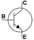
THE SYMBOL OF NPN BJT

image .

PNP TRANSISTOR

The other type of BJT is the PNP, consisting of a layer of N-doped semiconductor between two layers of P-doped material. A small current leaving the base is amplified in the collector output. That is, a PNP transistor is “on” when its base is pulled low relative to the emitter.
The arrows in the NPN and PNP transistor symbols are on the emitter legs and point in the direction of the conventional current flow when the device is in forward active mode.

THE SYMBOL OF PNP BJT.

image

CONNECTING BJT

The bipolar junction transistor, unlike LED, capacitor or resistor, it have three legs called as emitter (E), base (B) and collector (C). This means that interchanging the collector and the emitter of the transistor may leave the circuit not working.

CONNECTING NPN BJT
                                                     
I have marked the  collector (C), base (B) and emitter (E) pins on a real NPN BJT and also on the symbol

image

CONNECTING PNP BJT

I have marked the  emitter (E), base (B) and collector (C) pins on a real PNP BJT and also on the symbol

image

LIGHT DEPENDENT RESISTOR (LDR)

A light dependent resistor (LDR) or photoresistor or photocell is a resistor whose resistance decreases with increasing incident light intensity. Below I have shown LDR in different size (small to big).

image

In other words, LDR is a resistor whose resistance can be adjusted by the amount of light falling on it.

A photoresistor is made of a high resistance semiconductor. If light falling on the device is of high enough frequency, photons absorbed by the semiconductor give bound electrons enough energy to jump into the conduction band. The resulting free electron conduct electricity, thereby lowering resistance.

APPLICATIONS

Photoresistors can be found when we need to control some device with the variation in light.
Photoresistors come in many types. Inexpensive cadmium sulphide cells can be found in many consumer items such as camera light meters, street lights, clock radios, alarm devices, outdoor clocks, solar street lamps and solar road studs, etc.

SYMBOL OF LDR

image

CONNECTING LDR

LDR is also a two-terminal electrical which can be connected either way, that means it have no positive and negative terminal.

image

CAPACITOR

A capacitor is a two-terminal electrical component used to store energy electro statically in an electric field. When there is a potential difference across the conductors, an electric field develops across the dielectric, causing positive charge to collect on one plate and negative charge on the other plate. Energy is stored in the electrostatic field. In order to maximize the charge that a capacitor can hold, the dielectric material needs to have as high a permittivity as possible, while also having as high a breakdown voltage as possible.

In other words the capacitors act as a local reserve for the DC power source, and bypass AC currents from the power. Different types of capacitor is shown below

image

WHAT IS CAPACITANCE?

Capacitance is the ratio of the electric charge on each conductor to the potential difference between them. The SI unit of capacitance is the farad, which is equal to one coulomb per volt. An ideal capacitor is wholly characterized by a constant capacitance C, defined as the ratio of charge ±Q on each conductor to the voltage V between them.

CAPACITOR TYPES

Capacitors are available commercially in many different forms. Values range from very low picofarad range (ceramic capacitors) to about 5 kF (super capacitors).

CAPACITOR MARKINGS

Most capacitors have numbers printed on their bodies to indicate their electrical characteristics. Larger capacitors like electrolytic ones usually display the actual capacitance together with the unit (for example, .22 μF / 63V).

image

READING VALUE OF A CERAMIC CAPACITOR

Due to the smaller sizes of ceramics capacitors, there will be only three numbers and a letter, where the numbers show the capacitance in pF

Let’s calculate the value of the ceramic capacitors shown below

image

Calculated as XY × 10Z for the numbers XYZ and the letter indicates the tolerance.

A capacitor with the text 104K on its body has a capacitance of 10× 104 pF = 100 nF

APPLICATIONS

Energy storage
A capacitor can store electric energy when disconnected from its charging circuit, so it can be used like a temporary battery.

Capacitors are commonly used in electronic devices to maintain power supply while batteries are being charged.

In car audio systems, large capacitors store energy for the use of amplifier on demand.
The capacitors act as a local reserve for the DC power source, and bypass AC currents from the power.

CONNECTING CAPACITOR

A capacitor is a two-terminal electrical component.

The ceramic capacitors can be connected either way, that means it have no positive and negative terminal. The symbol used for the ceramic capacitors in a circuit diagram is:-

image

The electrolytic capacitors have a positive terminal (longer leg) and negative terminal (shorter leg) like one I marked below

image

The symbol used for the electrolytic capacitors in a circuit diagram is:

image

HAZARDS AND SAFETY

Capacitors may retain a charge long after power is removed from a circuit; this charge can cause dangerous or even potentially fatal shocks or damage connected equipment. So handle higher value capacitor with care.